Why Are Chipmakers Making Smaller and Smaller Processors?
If you’re a hardware enthusiast who’s been keeping a finger on the pulse of the industry, you’ve probably already heard or read the news around postponing the launch of the new 10nm chipsets again, which were slated for a 2016 release.
But first, what do those numbers really mean? In short, not much today—it’s become a little more than a marketing term, kept around to inform consumers that the industry has indeed been moving forward. Historically, however, that has not been the case. These numbers go by many names, some prefer to call them process technology, others process node, or even just node. They used to be tied to the parameters of transistors on a chip, such as gate length and minimum metal pitch, which traditionally were proportional to transistor size.
Moore’s Law predicted that transistor density on integrated circuits would double every 24 months. To achieve that, the components of the transistors had to shrink by a factor of 0.7 each node, and thus the names of the nodes were established. However, as foundries adopted newer, more sophisticated transistor designs, aforementioned parameters stopped being the driver of die shrink. In fact, there were nodes where the gate size stayed constant while everything else on the transistor shrunk, allowing foundries to fabricate denser chips.
Shallow as they may be, process nodes still do a good job as indicators to highlight generational leaps in the semiconductor industry. While some chipmakers haven’t been successful with the 10nm node, manufacturers focused on the mobile business have already produced commercially available 10nm products.
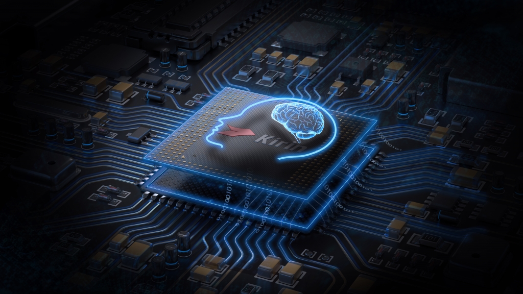
TSMC, for instance, manufactured the 10nm Kirin 970 SoC that is powering Huawei’s flagship devices: the HUAWEI Mate 10 Series and HUAWEI P20 Series. Soon, however, 10nm will cede its “cutting-edge” title to 7nm.
Generally, a denser chip equates to better performance and power efficiency. The former is driven by faster switching transistors, and the latter is due to a lower resistance and therefore lower current requirement for switching the transistors. Furthermore, the less power a chip consumes, the less heat it generates. Thermal performance is critical to ensuring a good smartphone user experience—a hot device is not only uncomfortable on the hand,but also could lead to processor throttling, which could severely hamper the performance of a device, leading to a subpar experience.
Additionally, moving to a smaller node enables a foundry to fabricate chips that are smaller, something that is extremely attractive to some of the foundry’s biggest customers: smartphone manufacturers. In smartphone design, every tiny bit of space is a precious commodity. A smaller chip could enable a handset maker to shave an additional half a millimeter off a device’s thickness or make space for a slightly larger battery. Alternatively, smaller chips enable chip designers to integrate additional processor units, such as AI processors, ISPs andDSPs, or simply pack more transistors into a SoC to bolster its features. Also, a smaller chip requires less raw material to manufacture, translating to lower manufacturing cost.
Looking back tothe short history of smartphones, we can see the semiconductor industry has always been the driver of innovation. It only took the industry six years to go from the 40nm K3V2 to the latest 7nm chip that Huawei is planning to unveil soon (more on this later). For better or worse, the performance of the chipset has always been the ceiling of smartphone capabilities—displays, cameras and graphical performance of devices are all limited by the performance of the SoC. But as chipsets become more advanced, the feature set of smartphones will only get richer as time goes on.
Until transistors reach the size of an atom, there will always be ways to shrink them down further. Currently, TSMC already has a roadmap that goes all the way down to the 3nm process. Many technology companies are already eyeing to migrate to 7nm and leverage its improved performance and efficiency to run process-intensive tasks such as AI, VR, AR and blockchain-based workloads. With the TSMC’s 7nm processors entering mass production in June 2018, devices carrying the new 7nm chips will likely hit the market soon.
According to Mr. Richard Yu, the CEO of Huawei CBG, Huawei will unveil the Kirin 980 at IFA, which will be the first commercially available 7nm chip in the world. The Kirin 980 will power the Mate 20 Series.
While the actual specifications of the Kirin 980 have not been announced yet, we can get a rough idea of its performance by reading TSMC’s official website, which states the foundry’s 7nm technology improves processor speed by approximately 20 percent and consumes approximately 40 percent less power compared to its 10nm counterpart.
Huawei has a stellar track record of leading chipset development. With Kirin 950, Huawei was the first to launch a 16nm chip, which came at a time when other manufactureswere designing chips for the 20nm process.
Huawei’s next device could well be the best Android device to come out in 2018. HUAWEI Mate 20 will launch with the world’s first 7nm chipset this October—consumers won’t have to wait much longer to experience the power of a next generation processor.


